


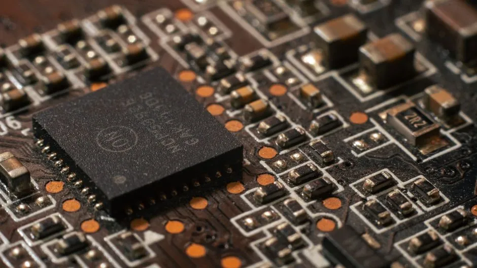
For decades, the semiconductor industry has operated on a simple, predictable rhythm: every couple of years, chips get smaller, faster, and more efficient. That rhythm, famously known as Moore’s Law, has powered everything from the first pocket calculators to the smartphones in our pockets. But lately, that rhythm has started to falter. As transistors shrink to the atomic scale, engineers are running into hard physical walls. Heat dissipation, electrical resistance, and manufacturing precision are making traditional scaling increasingly difficult. Enter Pat Gelsinger, Intel’s CEO, who believes the solution isn’t to push electrons harder, but to replace them with something fundamentally different: light.
The Physical Limits of Traditional Silicon
Modern computer chips rely on the flow of electrons through microscopic copper pathways. As these pathways shrink, they generate immense heat and suffer from signal interference. Moving data across a traditional silicon die is no longer as efficient as it used to be, and the power required to keep these systems cool is becoming a massive bottleneck. This is especially problematic for artificial intelligence, which demands staggering amounts of compute power and rapid data transfer between memory and processing units. When the hardware can’t keep up with the software’s appetite, innovation stalls.
Why Light Is the Next Big Leap
Instead of forcing more electrons through narrower channels, Gelsinger and his engineering teams are turning to silicon photonics. In simple terms, this technology uses microscopic beams of light to transmit data instead of electrical currents. Photons don’t generate heat the way electrons do, they don’t suffer from electrical resistance, and they can carry vastly more information at once. By routing data through optical waveprints etched directly into silicon chips, engineers can dramatically increase bandwidth while cutting power consumption. Think of it as upgrading from a narrow, congested two-lane road to a multi-level highway that moves traffic in all directions simultaneously.
Speed, Efficiency, and the AI Boom
The shift to optical interconnects isn’t just a nice-to-have upgrade; it’s a necessity for the next generation of artificial intelligence. Large language models and generative AI systems require trillions of calculations per second. Traditional copper wiring simply cannot move data between chip cores and memory fast enough without creating thermal bottlenecks. Optical computing bridges that gap. By enabling faster, cooler, and more energy-efficient data movement, light-based architecture gives AI workrooms the breathing room they need to scale without melting the data centers they run in.
Pat Gelsinger’s Strategic Pivot
Gelsinger’s vision goes beyond a single product launch. He sees optical integration as the foundation for reviving Moore’s Law in a new form. Rather than relying solely on shrinking transistor sizes, Intel is focusing on advanced packaging, three-dimensional chip stacking, and photonic interconnects to keep performance climbing. This approach allows the company to deliver exponential gains in computing density without waiting for breakthroughs in atomic-scale lithography. It’s a pragmatic, engineering-driven strategy that acknowledges the limits of physics while actively working around them.
The Roadblocks Ahead
Of course, transitioning from electrical to optical computing isn’t as simple as flipping a switch. Integrating photonic components into existing CMOS manufacturing lines requires entirely new fabrication techniques, specialized materials, and rigorous testing protocols. Optical chips also face challenges with signal loss, alignment precision, and cost efficiency at scale. Gelsinger has been transparent about these hurdles, noting that widespread adoption will take years of iterative development. Still, the foundational research is already showing promising results in lab environments, and several major tech players are investing heavily in similar photonic roadmaps.
What This Means for the Future of Computing
If successful, this shift will reshape how we think about hardware design. We’re moving away from an era defined by smaller transistors and into one defined by smarter architecture. Optical computing doesn’t just make chips faster; it makes them sustainable. Lower energy consumption means greener data centers, reduced cooling costs, and hardware that can handle increasingly complex AI workloads without straining global power grids. For developers, researchers, and everyday users, the end result will be more responsive devices, more capable AI assistants, and technology that simply keeps pace with ambition.
The age of purely electrical silicon may be reaching its practical limits, but the story of computing is far from over. By harnessing the speed and efficiency of light, Pat Gelsinger and Intel are laying the groundwork for a new chapter in semiconductor innovation. It won’t happen overnight, and the engineering challenges are real, but the direction is clear. As artificial intelligence continues to push the boundaries of what machines can do, light might just be the spark that keeps the entire industry moving forward.
